This 2-part blog series was inspired by a live presentation delivered at The Battery Show North America on October 8, 2025
Live Presentation

Agnes Sowa
India can skip over the decades and billions of dollars that its peers invested to develop the cutting-edge smart manufacturing technologies that are best practice today. In doing so, new semiconductor factories in India, both wafer fab and packaging, can enjoy improved time to market while optimizing yield, cost, and output. In short, India’s semiconductor industry can benefit from the collective work, investment and learnings of the rest of the world to build the smartest, most productive factories, building the highest quality products at the lowest cost. They can shift the S-curve, as we say, to produce more good die at every stage of the factory lifecycle.
In this first blog, we’ll look at the origins of manufacturing and what it means to make it “smart.”
Background
From semi to battery
Automotive’s inflection point
The automotive space is going through an inflection point. Cars are becoming more like the electronics we all know and love (or hate) in a shift visible in today’s software-defined vehicles. Today a car rolling off the assembly line with a fixed manufacturing bill of materials (MBOM) is capable of evolving its features post-sale. You can purchase a car and, two months later, subscribe for a few hundred dollars to unlock self-driving capabilities—enabled remotely by the manufacturer.
Typical new vehicles contain thousands of computer chips and millions of lines of code. The software and electronics are no longer just components, but integral to what drivers love about their cars. In essence, cars are becoming iPhones on wheels, with EV battery cells sharing many similarities with computer chips inside personal devices. Both are hybrids of chemical and physical properties that together determine performance.
The process used to manufacture battery cells also mirrors that of semiconductors: a continuous flow that transitions into batch processing and ultimately results in discrete units. Both industries demand highly controlled environments—dry rooms, clean rooms, and precise environmental controls integrated with Manufacturing Execution Systems (MES), Statistical Process Control (SPC), and process data.
Shared challenges: precision and loss minimization
Failure in either domain—semiconductors or batteries—leaves little room for rework. There are no easy reentry loops. That’s why both industries focus intensely on minimizing losses and waste.
Fault detection and classification entails looking at the combination of physical, chemical, and visible inspection data combined with equipment sensor data to conduct classification and detection. In wafer fabs, however, this is done at a much higher scale and volume of data. A typical tech stack for a semi wafer fab, as shown in figure 1, has everything necessary to run lights out manufacturing. This includes automation of material movements, the manufacturing execution system, process quality, productivity (including scheduling), asset management, and preventive maintenance. It is the soup-to-nuts solution for a wafer fab.
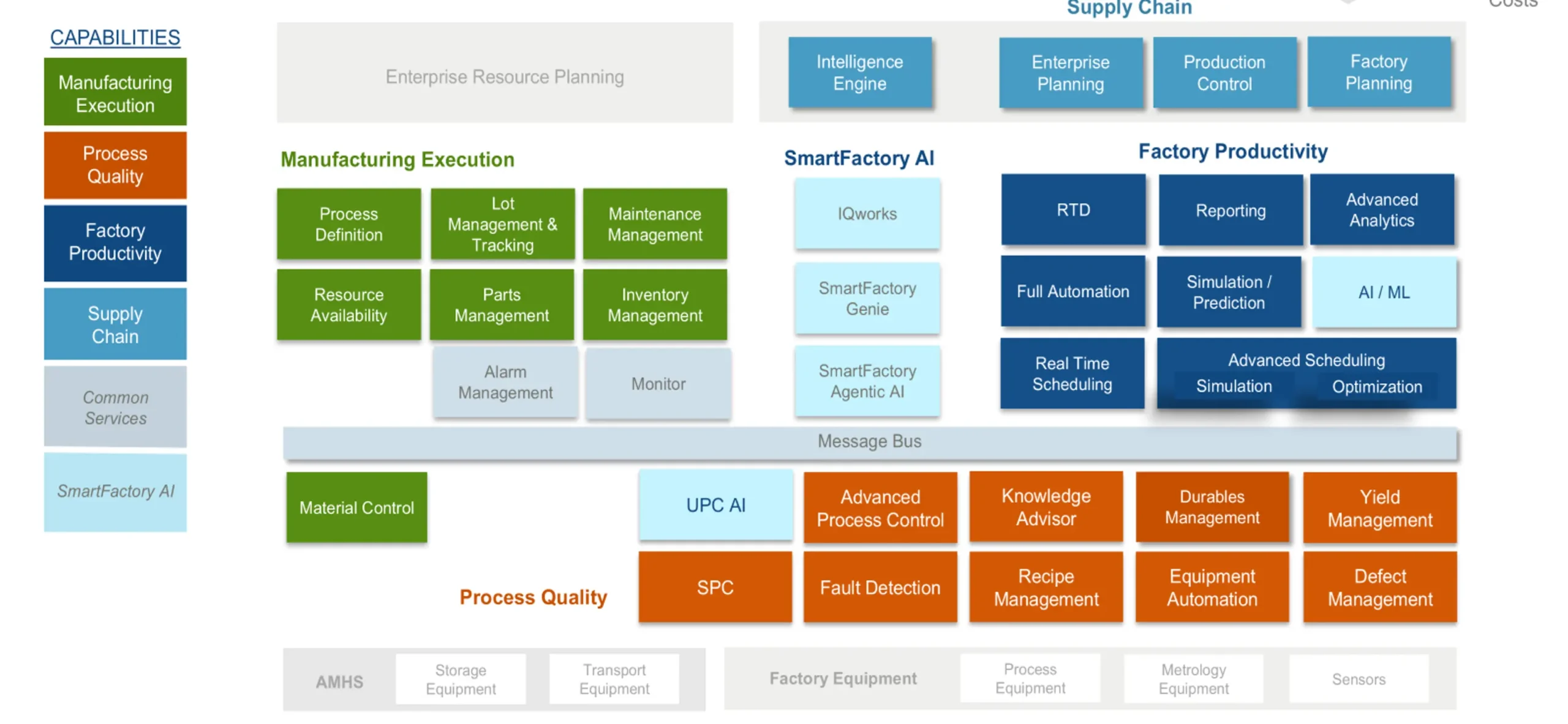
For the moment, we’ll just look more closely at process quality solutions within this stack, and how they can bring about savings to the giga factory via improved process quality: SPC, fault detection (FD), and predictive maintenance.
SPC and FD: what and why
Simply put, SPC will answer your ‘what.’ Fault detection will answer ‘why,’ and predictive maintenance will tell you how and when.
Both wafer fabs and giga factories frequently employ SPC for monitoring process limits and maintaining control. This standard use of SPC typically involves advanced process controls, out of control action plans (OCAP), and analysis of process trends. Control charts serve as time series data, essentially identifying your set limits and revealing how your process is performing at present.
Fault detection is also used to answer why incidents occur. When process drift occurs, such as a sequence of points with measurement anomalies, you might look at a burr count after electrode slitting. The FD system, on the other hand, monitors equipment sensors and begins observing parameters such as roller tension which might contribute to burr formation in slitting. Additionally, it examines other critical data to help correlate and determine the underlying reasons for process failures at the conclusion of processing.
This use of FD still tends to be very reactive, initiated only when the process engineer first identifies an issue. Fault detection is a familiar and intuitive tool for process engineers. It relies on time series data and, since the process is highly continuous, unit IDs aren’t present at this stage. What they’ll typically see is a chart with the mean and the sigma, max, and range. While they’ll be able to identify outliers, further analytics such as calculating slope and combining sensor signals into composite indices allow for extra computational insights to help determine underlying causes—the why. As with SPC, however, this method remains mostly reactive as it is typically performed after a failure occurs on the process side.
Prevention
FD is also an essential tool that enables manufacturers to begin to predict or even prevent future failures. The level of data it generates can be used in unison by process and quality and maintenance teams to extrapolate when a threshold likely to cause a failure will be crossed. Identifying time to failure (the time from now until the threshold will be reached) enables preventive maintenance to be planned first.
This is likely a process used by most battery gigafactories, albeit through manual actions. Working with customers, we found many built preventive maintenance schedules through a mix of vendor consultations, input from process engineers, and accumulated best practices—layered with whatever connected data fed into preventive maintenance—all aimed at devising the most effective predictive maintenance schedule possible for their organization.
Predictive maintenance
To move away from these manual processes to optimize the benefits of preventive maintenance, we developed the Anomaly Detection Ensemble (ADE) solution. Through a series of machine learning algorithms, it produces an extrapolation with a confidence window that results in a much tighter window of maintenance intervals on the time axis. This enables process engineers to take more risks when rescheduling preventive maintenance—to extend the time between maintenance events. In terms of operational benefit, manufacturers can schedule maintenance further into the future and gain more equipment up time.
Up next: how
While all these individual solutions have been around, what is innovative is how wafer fabs have done this. This can be summed up in two points: having a common software platform that is looking at that time series data from the perspective of your process engineer, and presenting that data in a way your process engineers know how to interpret. This automates the connection between why your maintenance team is taking certain actions and prioritizing those — aligning their objectives to quality objectives. In the next article, we’ll share a case study demonstrating how this type of implementation can make these practices systemic and enable significant savings in the process.